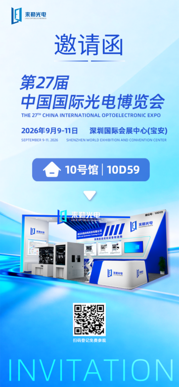
The China International Optoelectronic Exposition (CIOE) is the world's largest and most influential comprehensive exhibition in the optoelectronics industry. The 27th China International Optoelectronic Exposition (CIOE 2026) will be grandly held from September 9 to 11, 2026, at the Shenzhen World Exhibition & Convention Center.
Global investment in AI computing power continues to rise, driving the large-scale production and deployment of 800G and 1.6T high-speed optical modules. As core manufacturing support for the optical interconnection industry, packaging equipment is undergoing a comprehensive acceleration in domestication and automation upgrades.
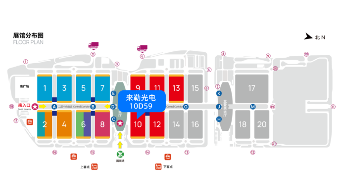
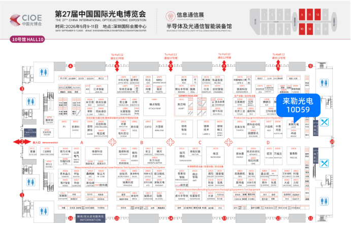
At this exhibition, Laile Optoelectronics will showcase multiple devices in Shenzhen, sincerely inviting industry colleagues as well as new and existing customers to visit Hall 10, Booth 10D59, to jointly explore the iteration of 800G/1.6T mass production processes and development opportunities in the AI computing optical interconnect industry.
Core Product
Dual-Lens Automatic Coupling Packaging System
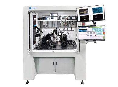
Laile Optoelectronics' self-developed dual-lens automatic coupling equipment is used for lens coupling and optical path shaping. The equipment primarily enables coupling and packaging between LD, single-lens, dual-lens, FA/fiber. It features a dual-sided electric six-axis design, supporting single-sided and dual-sided coupling. The equipment is equipped with high-precision image recognition and positioning functions, achieving automated material loading, automatic dispensing, and automatic UV curing. By updating the fixtures, it can accommodate various specifications of lenses and devices, offering convenient operation and significantly improving production efficiency.
Dual FA Automatic Coupling System
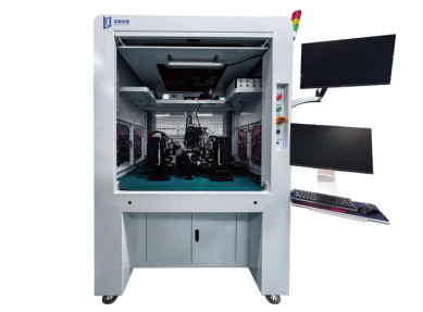
The dual FA automatic coupling system is a dual FA automatic coupling device independently developed by our company, compatible with both TX and RX ends. It features high-precision image recognition and positioning capabilities, can automatically adjust the relative parallelism between the PCB board and the FA, and simultaneously perform end-face coupling between the TX end and the FA, as well as vertical coupling between the RX end and the FA, with automatic adhesive dispensing and curing. This equipment is suitable for a variety of materials, including silicon photonics, thin-film lithium niobate, and III-V semiconductors.
COB Automatic Coupling System
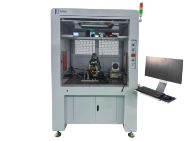
The COB automatic coupling system is a COB coupling device independently developed by our company, featuring one-button operation, easy loading, and high-precision image recognition and positioning capabilities. It is suitable for multi-mode 850nm wavelength active COB products, such as 400G/800G SR4/SR8 optical modules. The equipment can automatically identify the position and angle of PCB boards and lens materials, perform automatic coupling with an efficiency of less than 60 seconds, and also supports functions such as automatic dispensing and UV curing. The device is easy to operate, highly automated, and offers excellent consistency.
Fully Automatic Coupling Equipment for Pump Lasers
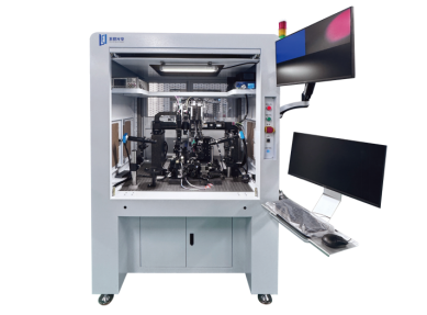
The Pump laser coupling system is an automatic coupling device independently developed by Wuhan Laile Optoelectronics Technology Co., Ltd., based on butterfly package devices. It is an automatic coupling device used for inserting optical fibers into the interior of the butterfly package for coupling. The device features image recognition and positioning functions, can precisely adjust the position of materials, and can achieve automatic coupling alignment, automatic dispensing, and automatic curing functions.
Chip Testing System
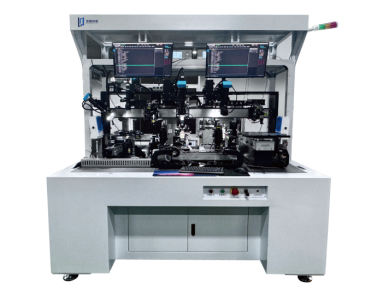
The chip testing system is a testing platform independently developed by Wuhan Lailer Optoelectronics Technology Co., Ltd., primarily used to perform forward and backward optical and electrical performance tests on CHIP semiconductor laser chips. It can also integrate spectral measurements and consolidate outputs such as LIV, spectral data, and divergence angle data. The equipment is widely used for mass production testing of chips such as DFB and EML.
Silicon Photonics Chip Automatic Coupling Testing System
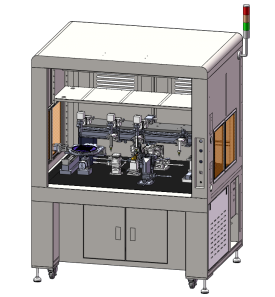
The silicon photonic chip automatic coupling test system can simultaneously meet the requirements for chip coupling and testing. The system supports coupling tests for different types of chips, bars, and wafers, with flexible parameter settings, a visualized interface, and convenient operation. This equipment is suitable for coupling tests of various materials, including silicon photonics, thin-film lithium niobate, and III-V compounds.
We are here